Export souborů z KiCad » Historie » Revize 1
Revize 1/5
| Další »
Aleksei Karavaev, 2020-09-27 13:44
Export souborů z KiCad
Select File -> Plot.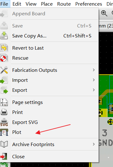
Potřebujete mit vybrano alespon 8x vrstev:
Top Copper (F.Cu)+ Soldermask (F.Mask) + Silkscreen (F.SilkS)
    Bottom Copper (B.Cu) + Soldermask (B.Mask) + Silkscreen (B.SilkS)
    Board outline (Edge.Cuts)

Drill file
In the Plot window with the Plot format set for Gerber, be sure these Layers are checked:
If you don't know which layers, please check all layers, JLCPCB will help you to use the right layers. Click ‘Plot’ to generate the gerber files for the layers.
Don't forget to Generate the Drill Files. Click on ‘Generate Drill File’ button. You can use the defaults here as well. Check the "Merge PTH and NPTH holes into one file" box. For now just click ‘Drill File’ or press ‘enter’ to generate the drill file. Use the same output folder as for the gerbers, which should be the default.
Check the Gerber files in GerbView
Next, click ‘Close’to exit the Drill and Plot windows. All of the files should have appeared in your gerbers folder. KiCAD comes with a gerber viewer called GerbView, you can open the “GerbView” and check what your board looks like before sending it to manufacturer.
Aktualizováno uživatelem Aleksei Karavaev před více než 5 roky(ů) · 5 revizí